3D IC 바카라사이트 쿠폰 시장 규모 및 점유율
시장 개관
| 학습 기간 | 2019 - 2030 |
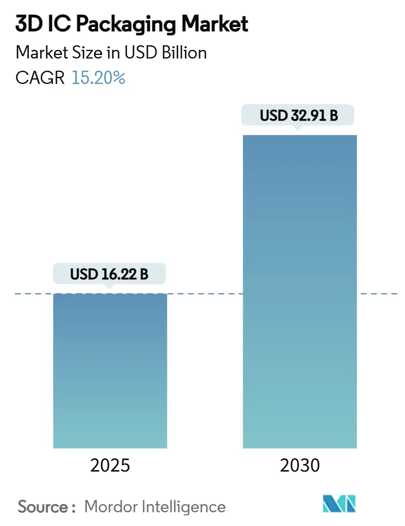
| 시장 규모(2025년) | USD 16.22 십억 |
| 시장 규모(2030년) | USD 32.91 십억 |
| 성장률(2025년~2030년) | 15.20 % CAGR |
| 가장 빠르게 성장하는 시장 | 중동 및 아프리카 |
| 가장 큰 시장 | 아시아 태평양 |
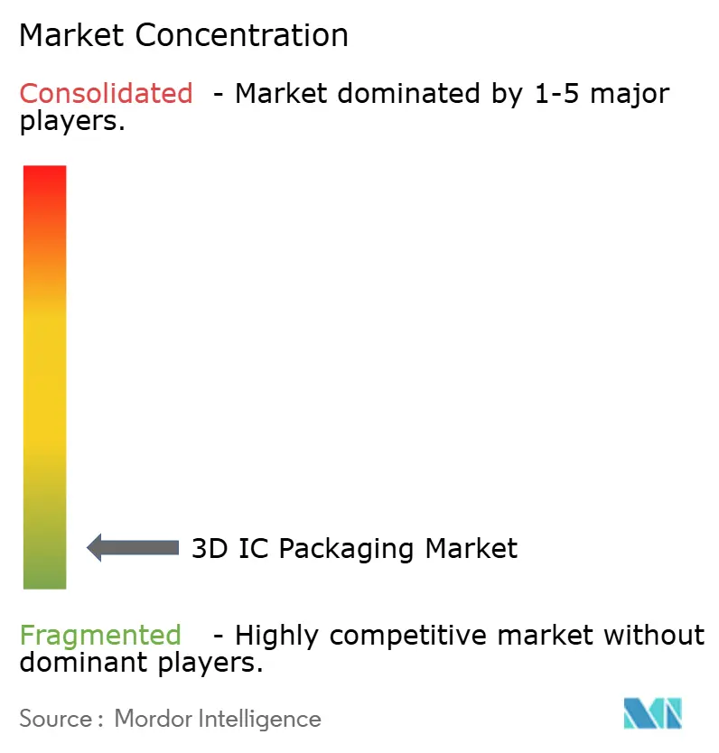
| 시장 집중 | 높음 |
주요 선수
*면책조항: 주요 플레이어는 특별한 순서 없이 정렬되었습니다. 이미지 © 바카라 사이트. 재사용 시 CC BY 4.0에 따라 저작자 표시가 필요합니다. |
|
바카라 사이트의 3D IC 바카라사이트 쿠폰 시장 분석
3D IC 바카라사이트 쿠폰 시장 규모는 16.22년 2025억 32.91천만 달러로 추산되며, 2030년까지 15.2억 2025천만 달러에 이를 것으로 예상됩니다. 이는 2030년부터 2년까지 연평균 4% 성장한 수치입니다. 이러한 급증은 기존 3D 레이아웃의 대역폭, 지연 시간 및 전력 한계를 뛰어넘는 인공지능 및 고성능 컴퓨팅 워크로드 급증에 힘입어 반도체 공급업체들이 수직 적층 아키텍처를 채택하도록 강요하고 있습니다. XNUMXD IC 바카라사이트 쿠폰 시장에서 HBMXNUMX+와 같은 첨단 메모리 및 로직-메모리 공동 설계는 비용 계층 구조를 재정립하고 있으며, TSV(Through Silicon Via) 툴링 및 CoWoS 기판의 수급 불균형은 단기 생산량 증가를 저해하고 있습니다. 아시아 태평양 지역은 대만과 한국의 긴밀하게 통합된 파운드리 클러스터 덕분에 압도적인 선두를 유지하고 있지만, CHIPS법에 따른 북미 리쇼어링과 걸프 지역 그린필드 프로그램으로 인해 장기적인 생산 능력 체계가 변화하고 있습니다. 수출 통제 체제 강화와 국방 수준의 보안 의무화로 인해 파운드리 업체들은 수율 확보에 차질을 빚지 않으면서 장비 조달 및 파트너 네트워크를 재설계해야 합니다.[1]정팅팡, “TSMC, 엔비디아, 구글 AI 칩용 차세대 바카라사이트 쿠폰에 한발 더 다가가다”, 닛케이아시아, asia.nikkei.com
주요 바카라 요약
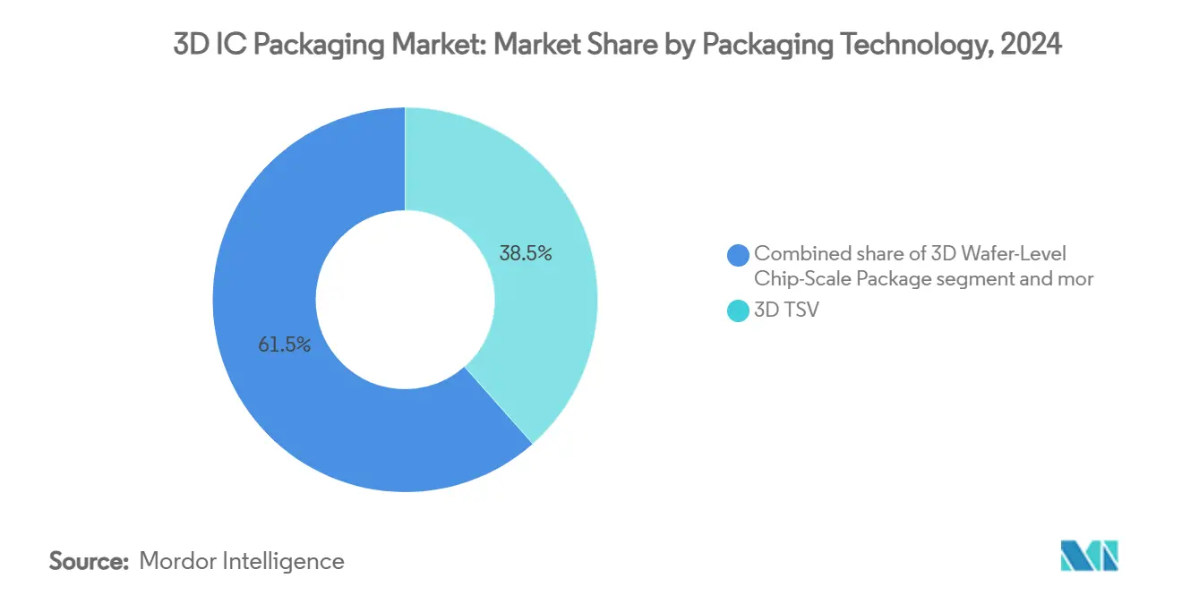
패키징 기술별로 보면, 3D TSV는 38.46년에 3D IC 바카라사이트 쿠폰 시장 점유율 2024%를 유지했고, 하이브리드 본드 스태킹은 21.73년까지 연평균 성장률 2030%로 증가할 것으로 예상됩니다.
통합 방식에 따르면, 2.5D 인터포저는 58년에 3D IC 바카라사이트 쿠폰 시장에서 2024%의 점유율을 차지했으며, 진정한 3D 스태킹은 22.09년까지 2030%의 CAGR로 가장 가파른 성장을 보였습니다.
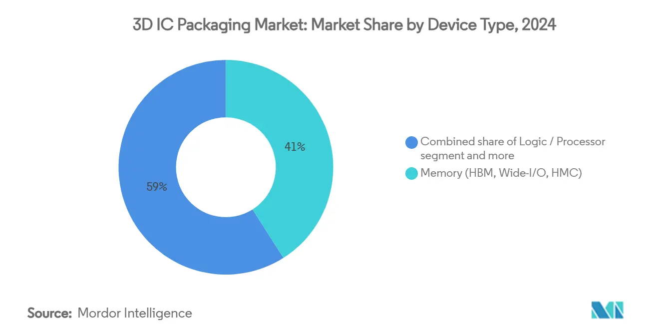
장치 유형별로 보면, HBM 스택이 주도하는 메모리는 41년 3D IC 바카라사이트 쿠폰 시장 규모의 2024%를 차지했습니다. HBM4+ 물량은 24.91년까지 2030%의 CAGR을 기록할 것으로 예상됩니다.
최종 사용자 애플리케이션별로 보면, HPC와 AI는 38년에 3D IC 바카라사이트 쿠폰 시장에서 2024%의 수익 점유율을 차지했으며 19.77년까지 2030%의 CAGR을 기록할 것으로 예상됩니다.
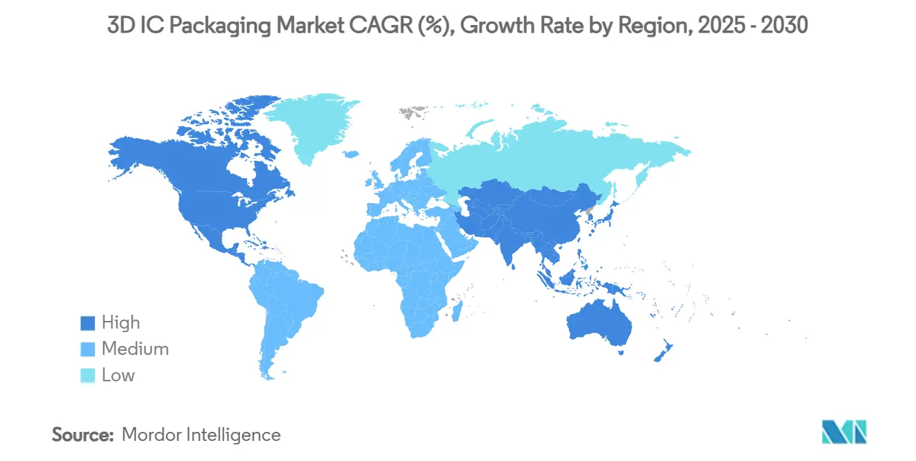
지역별로 보면 아시아 태평양 지역이 63년 2024%의 점유율로 19.79위를 차지했고, 중동 및 아프리카 지역은 2025년부터 2030년까지 XNUMX%의 CAGR을 기록할 것으로 예상됩니다.
글로벌 3D IC 바카라사이트 쿠폰 시장 동향 및 통찰력
드라이버 영향 분석
| 운전기사 | (~) CAGR 예측에 미치는 영향 | 지리적 관련성 | 영향 타임라인 |
|---|---|---|---|
| HBM 적층 패키지에 대한 폭발적인 AI/HPC 수요 | 4.20% | 글로벌, 북미 및 아시아 태평양 지역에 집중 | 단기 (≤ 2년) |
| 모바일 및 웨어러블, 웨이퍼 레벨 칩 스케일 패키지(WLCSP)로 전환 | 2.80% | APAC 핵심, 북미로의 스필오버 | 중기(2~4년) |
| 파운드리 "파운드리 2.0" 전략, 바카라사이트 쿠폰 통합 | 2.10% | 대만과 한국이 주도하는 글로벌 | 중기(2~4년) |
| 유리 코어 및 패널 수준 기판으로 규모에 맞춰 비용 절감 | 1.90% | APAC 제조, 글로벌 배치 | 장기 (≥ 4년) |
| 방어용 칩렛은 안전한 이기종 통합을 요구합니다. | 1.40% | 북미 및 EU, 선택적 APAC | 장기 (≥ 4년) |
| 저온 하이브리드 접합을 우선시하는 탄소 중립 팹 | 0.80% | EU 및 북미, APAC로 확장 | 장기 (≥ 4년) |
출처: 모르도르 정보
HBM 적층 패키지에 대한 폭발적인 AI/HPC 수요
데이터센터 가속기의 물결이 부품 목록(BOM)의 우선순위를 재편하고 있으며, 3D IC 바카라사이트 쿠폰 시장에서 HBM 스택이 모든 고급 노드 로드맵의 최상위로 부상하고 있습니다. TSMC는 엔비디아의 차세대 GPU와 보조를 맞추기 위해 88,000년까지 CoWoS 생산량을 월 2026만 3천 장으로 확대할 계획입니다. HBM4E에서 HBM3+로의 전환은 유효 대역폭 밀도를 세 배로 높이는 동시에 열 설계 한계를 일정하게 유지하여 기판 제조업체들이 더 두꺼운 코어 재료와 더 미세한 구리 재배선층을 확보하도록 강요하고 있습니다. 삼성의 H-Cube 플랫폼은 로직과 메모리를 패키지에 결합하여 메모리 중심 토폴로지가 보드 레벨 아키텍처로 어떻게 확장되는지를 보여줍니다. 그 결과, 디바이스당 적층 다이 비율(stacked-die ratio)이 높아지고, TSV 믹스가 더욱 풍부해지며, 궁극적으로 XNUMXD IC 바카라사이트 쿠폰 시장 전반의 평균 판매 가격이 상승합니다.
모바일 및 웨어러블, 웨이퍼 레벨 칩 스케일 패키지(WLCSP)로 전환
웨어러블 및 프리미엄 스마트폰 OEM들은 이제 웨이퍼 레벨 시스템 인 패키지(SiP) 방식을 무선 통신, PMIC, MEMS를 7mm 미만 플랫폼에 집적하는 기본 방식으로 보고 있습니다. 애플의 2026년 플래그십 모델은 A 시리즈 SoC용 고급 WLCSP를 선보일 것으로 예상되는데, 이는 폼팩터가 기존의 핀당 비용(CPC)을 능가하고 있음을 시사합니다. 대만 OSAT 업체들은 재배선층수(RDL) 우선 공정 전용 리소그래피 라인을 두 배로 증설하여 대응하고 있으며, 한국 경쟁사들은 휨 현상 완화를 위해 레진 코팅 구리 포일을 채택하고 있습니다. 이러한 움직임은 3D IC 바카라사이트 쿠폰 시장을 데이터 센터 실리콘을 넘어 일반 소비자 기기로 확장하여 수익원을 다각화하고 팹 로딩 팩터를 개선하고 있습니다.
파운드리 "파운드리 2.0" 전략, 바카라사이트 쿠폰 통합
노드 간 트랜지스터 증가율이 과거 기준치 이하로 떨어지면서 웨이퍼 제조와 첨단 바카라사이트 쿠폰의 경계는 사라졌습니다. TSMC의 65억 달러 규모 애리조나 캠퍼스는 현재 CoWoS와 SoIC 서비스 전용 건물 두 채를 운영하고 있습니다. 삼성의 로드맵은 2nm FEOL과 2.5D H-CUBE 백엔드를 동일한 클린룸 단지에 통합하여 공장 간 사이클 타임을 30% 단축합니다. 한편, 인텔 파운드리 서비스는 포베로스 다이렉트(Foveros Direct)와 EMIB를 레티클 스티칭 옵션과 함께 제공하여 고객이 최첨단 컴퓨팅 타일과 기존 I/O 다이를 결합할 수 있도록 지원합니다. 수직 통합은 마진을 높이고 수율 학습을 가속화하며, 파운드리를 3D IC 바카라사이트 쿠폰 시장 전체 라이프사이클을 위한 원스톱 솔루션으로 자리매김합니다.[2]플로라 왕(Flora Wang)과 징웨 샤오(Jingyue Hsiao), "C Sun, 미국 반도체 확장 열풍에 합류할 준비", DIGITIMES, digitimes.com
유리 코어 및 패널 수준 기판으로 규모에 따른 비용 절감
유기 기판은 ≥50Gbps 다이-투-다이 연결의 공면성 및 CTE 요건을 충족할 수 없으므로, 유리 관통 비아(TGV)를 지원하는 유리 코어 적층판의 조기 도입이 촉진되었습니다. 인텔의 2025년 파일럿 프로젝트는 40mm 유리 코어에서 스큐 분산(skew variance)이 300% 감소하는 것을 보여주었으며, 이는 510mm x 515mm 기판에 패널 레벨 스티칭을 가능하게 하는 기반을 마련했습니다. TSMC의 패널 레벨 바카라사이트 쿠폰 프로그램은 20년까지 AI 가속기의 단가를 30~2027% 절감하는 것을 목표로 하고 있으며, C Sun과 Mycronic은 대만 OSAT에 대형 리소그래피 장비를 공급하고 있습니다. 규모의 경제가 실현됨에 따라 유리 기반 캐리어는 2D IC 바카라사이트 쿠폰 시장의 3차 고객 기반을 확대할 것입니다.
방위 등급 칩렛은 안전한 이기종 통합을 요구합니다.
미국과 유럽 국방 기관들은 이제 개별 범프 형상까지 감사가 가능한 변조 방지형 멀티벤더 칩렛 스택을 지정하고 있습니다. 미국 SHIP 이니셔티브 기금 프로토타입 실행과 같은 프로그램에서는 신뢰할 수 있는 북미 팹에서 처리된 로직을 안전한 시설 내에서 아시아 태평양 지역에서 공급된 RF 다이에 하이브리드 본딩 방식으로 연결합니다. 신뢰할 수 있는 해외 공정, 안전한 펌웨어 프로비저닝, 그리고 수명 주기 추적성에 대한 요구는 단위당 엔지니어링 콘텐츠 수를 증가시키고 3D IC 바카라사이트 쿠폰 시장의 특수 분야에 프리미엄 가격을 부과합니다. 공급망 투명성 도구와 암호화된 다이 간 연결은 기계적 정렬 정확도만큼이나 중요해지고 있습니다.
제약 영향 분석
| 제지 | (~) CAGR 예측에 미치는 영향 | 지리적 관련성 | 영향 타임라인 |
|---|---|---|---|
| 생산 TSV 도구 및 CoWoS 용량 부족 | -3.10 % | 전 세계적으로 APAC에서 가장 심각함 | 단기 (≤ 2년) |
| 1W/mm²를 넘는 열 설계 한계(TDL) 과제 | -2.40 % | 글로벌, HPC 애플리케이션에 중요 | 중기(2~4년) |
| 3D 평면도에 대한 높은 IP/EDA 비용 | -1.80 % | 글로벌, 디자인 센터에 집중 | 중기(2~4년) |
| 초기 PLP 라인에서 패널 휘어짐 및 수율 손실 >3% | -1.20 % | APAC 제조 허브 | 단기 (≤ 2년) |
출처: 모르도르 정보
생산 TSV 도구 및 CoWoS 용량 부족
TSV 식각기, 본딩 얼라이너, CoWoS급 기판 라미네이터는 12~18개월 후에도 예약이 꽉 차 있어 AI 가속기 일정을 맞추기 위해 애쓰는 OSAT 업체들의 성장 잠재력을 제약하고 있습니다. 어플라이드 머티어리얼즈와 도쿄 일렉트론은 2026년 중반까지 두 자릿수 장비 수주 잔고를 예상하고 있지만, 부품 부족과 설치 인력 부족으로 실제 양산 속도가 느려지고 있습니다. TSMC가 CoWoS 기판 시장에서 가장 큰 점유율을 차지하고 있는 가운데, 구매자들은 웨이퍼 초기 물량을 확보하기 위해 경쟁하며, 때로는 분기별 물량을 선불로 지불하기도 합니다. 이러한 희소성으로 인해 수요 신호가 뚜렷하게 강함에도 불구하고 3D IC 바카라사이트 쿠폰 시장 전반의 즉각적인 매출 실현이 제한되고 있습니다.[3]“ASM International, 53.4년 14분기 AI 칩 주문 1% 급증에 따라 사상 최대 2025% 마진 달성” StockTitan, stocktitan.net
1W/mm²를 넘는 열 설계 한계(TDL) 과제
적층 다이가 1W/mm²를 초과함에 따라 기존 히트 스프레더는 중간층의 접합부 열을 배출하지 못합니다. TSMC는 실리콘 인터포저에 직접 식각된 미세유체 냉각 채널을 시범 적용하고 있지만, 초기 단계의 프로토타입은 제조 복잡성과 신뢰성 불확실성을 가중시킵니다. 따라서 소자 제조업체는 클럭 속도를 조절하거나 분산형 칩렛 레이아웃을 채택해야 하며, 이는 일부 성능 향상을 희석시키고 전력 예산을 증가시킵니다. 냉각 혁신과 전력 밀도 향상 간의 격차는 향후 3년 동안 지속될 것이며, XNUMXD IC 바카라사이트 쿠폰 시장의 복합 성장 궤도에서 포인트를 깎아낼 것입니다.
세그먼트 분석
바카라사이트 쿠폰 기술: TSV 리더십, 하이브리드 본딩 혁신에 직면
3D TSV 노드는 38.46년 3D IC 바카라사이트 쿠폰 시장 점유율 2024%를 유지했습니다. 이는 성숙한 리소그래피 규칙, 대량 생산 툴링, 그리고 현장 신뢰성 데이터가 메모리 공급업체의 GB당 비용 목표와 일치했기 때문입니다. 여러 HBM3E 라인은 이미 TSV 드릴 및 충진 장비의 비용을 상각하여 다이 수가 증가했음에도 불구하고 매출 총이익률을 안정적으로 유지했습니다. 그러나 하이브리드 본드 부문은 연평균 21.73%의 성장률을 기록하며 구리-구리 직접 접촉을 활용하여 z-높이를 40%, 상호 연결 저항을 15% 절감하고 있습니다. 이러한 전기적 이득은 기존의 패키지-기판 이탈 라우팅 한계를 뛰어넘는 컴퓨팅 집적도 높은 AI 가속기에 매우 중요합니다.
이러한 전환이 TSV를 쓸모없게 만드는 것은 아닙니다. 대신 이중 경로 로드맵이 등장합니다. TSV는 대용량 메모리 및 센서 스택의 기본으로 남아 있는 반면, 하이브리드 본딩은 3D IC 바카라사이트 쿠폰 시장에서 컴퓨팅 중심의 저지연성 영역을 점유합니다. 두 플로우를 인접 라인에서 모두 호스팅할 수 있는 OSAT는 위험 분산형 수주를 확보합니다. 기판 제조업체들이 유리 코어를 확장함에 따라 하이브리드 본딩 정렬 정확도가 더욱 향상되어, 비용 곡선이 교차하고 특정 볼륨 SKU에서 하이브리드 본딩이 TSV를 대체하는 미래 교차점을 예고합니다.
참고: 바카라 구매 시 사용 가능한 모든 개별 세그먼트의 세그먼트 공유
통합 접근 방식: 진정한 3D 진화로 인해 인터포저 지배력에 도전받다
2.5D 인터포저는 58년 매출의 2024%를 기록하며, 실리콘 인터포저 결함률을 0.1dpm 미만으로 낮춘 3년간의 수율 학습을 활용했습니다. 인터포저는 프런트엔드 노드 선택과 백엔드 조립을 분리하기 때문에 GPU 공급업체는 전체 스택을 재설계하지 않고도 기존 노드의 I/O 다이 옆에 레티클 크기의 컴퓨팅 타일을 제공합니다. 그러나 진정한 22.09D 스태킹은 다이 간 지연 시간 증가로 인해 모델 학습 시간을 두 자릿수 비율로 단축할 수 있어 XNUMX%의 CAGR을 기록합니다. 주요 사용 사례로는 수직 NAND, 메모리 기반 컴퓨팅 렌즈, 패키지 내 고Q RF 필터 등이 있으며, 이는 모두 z축 근접 방식이 평면 레티큘레이션 방식보다 우수한 시나리오입니다.
초기 신뢰성 우려(매립된 마이크로 범프에서의 전기적 이동 및 다이 모서리에서의 열-기계적 전단)는 저탄성 언더필과 하이브리드 본드 구리 확산 배리어를 통해 완화되고 있습니다. 마이크로 유체 냉각 및 그래핀 열 분산기가 성숙함에 따라 진정한 3D 채택이 가속화되고 있습니다. 따라서 3D IC 바카라사이트 쿠폰 시장은 인터포저 주류와 진정한 적층 성능 우위로 양분되며, 각각 가격만이 아닌 차별화된 KPI 로드맵을 기반으로 발전하고 있습니다.
장치 유형별: 메모리 애플리케이션이 HBM4+ 혁신을 주도합니다
메모리는 41년 매출의 2024%를 차지하며 3D IC 바카라사이트 쿠폰 시장에서 단일 최대 사용량을 기록했습니다. 4년 대량 생산을 목표로 하는 HBM2027+로의 전환이 임박함에 따라 메모리 중심 패키지 시장은 24.91년까지 연평균 2030% 성장할 것으로 예상됩니다. 적층형 메모리 공급업체들은 파운드리 파트너와 채널 아키텍처 및 마이크로 범프 피치를 공동 설계하여 1Tbps 이상의 총 대역폭에서 신호 무결성을 유지합니다. 로직과 메모리를 결합한 코본드는 SKU별로 상충 관계를 발생시킵니다. 레이어 수가 많을수록 캐시 상주 시간은 늘어나지만, 열 관리 예산은 더 어려워집니다.
메모리 외부에서 로직 프로세서는 EUV 패턴의 컴퓨팅 타일과 성숙 노드 PHY 다이를 혼합하는 칩렛 파티셔닝을 통해 시장 점유율을 확대합니다. 센서 및 MEMS 모듈은 3D WLCSP를 채택하여 웨어러블 기기 및 자동차 실내 공간에 치과용 페이스트 크기의 패키지로 광학, 관성 및 환경 감지 기능을 통합합니다. RF 및 아날로그 플레이어는 유리 코어 내부의 수직 절연을 활용하여 5G FR2 주파수가 52GHz를 초과하는 경우에도 노이즈에 민감한 블록을 보호합니다. 각 디바이스 하위 틈새 시장은 3D IC 바카라사이트 쿠폰 시장에서 자체적인 비용 대비 성능 범위를 형성하여 수요 다변화를 촉진하고 용량 활용도를 원활하게 합니다.
참고: 바카라 구매 시 사용 가능한 모든 개별 세그먼트의 세그먼트 공유
최종 사용자 애플리케이션별: HPC 및 AI 지배력으로 산업 우선순위 재편
HPC 및 AI 워크로드는 38년 매출의 2024%를 차지했으며, 19.77년까지 연평균 성장률 2030%로 성장할 것으로 예상되어 가속기 공급업체를 패키지 기판 할당 부문의 최상위 계층으로 끌어올릴 것입니다. 클라우드 하이퍼스케일러는 상용 실리콘을 점점 더 피하고 CoWoS 또는 패널 단위 캐리어에 내장된 맞춤형 ASIC에 투자하여 3D IC 바카라사이트 쿠폰 시장에서 확실한 슬로팅을 확보하고 있습니다. 모델 매개변수 수가 XNUMX개월마다 두 배로 증가함에 따라, 기판 XNUMXmm당 대역폭은 무어 시대의 트랜지스터 밀도를 능가하는 핵심 지표가 되었습니다.
가전제품은 규모 모멘텀을 유지하고 있습니다. 특히 OEM 업체들이 스마트폰에 혼합 현실 컴퓨팅을 추가함에 따라 이러한 모멘텀이 유지되고 있지만, 가격 경쟁력은 데이터센터 평균 판매 가격에 비하면 미미합니다. AEC-Q100과 ISO 26262가 적용되는 자동차 및 ADAS 설계는 -40°C에서 150°C까지의 온도 범위에서 긴 작동 시간을 요구하며, 이는 공급업체들이 온도 사이클링에 강한 언더필 화학 물질을 채택하도록 유도합니다. 항공우주 및 방위 산업은 안전한 칩렛과 방사선 내성 유전체를 채택하여 제곱밀리미터당 소비자 평균 판매 가격의 3~5배를 지불합니다. 의료 및 산업용 IoT 패키지는 광자 센서와 초저누설 로직을 우선시하여 3D IC 바카라사이트 쿠폰 시장의 기술적 우위를 약화시키지 않으면서 시장 점유율을 확대합니다.
지리 분석
아시아 태평양 지역은 63년 3D IC 바카라사이트 쿠폰 시장의 2024%를 점유했는데, 이는 대만의 첨단 노드 패권, 한국의 메모리 중심 백엔드 클러스터, 그리고 중국의 국내 생산 능력 확대에 따른 결과입니다. TSMC의 CoWoS, 삼성의 H-Cube, 그리고 ASE의 FOCoS 플랫폼은 밀집된 공급업체 네트워크를 기반으로 물류 지연 시간을 단축하고 공정 전환 루프를 빠르게 진행합니다. 그럼에도 불구하고, 지정학적 역류로 인한 이전 위험으로 일부 고객은 말레이시아, 싱가포르, 베트남으로의 이중 소싱을 선택하게 되었고, 이는 이 지역의 기술 도달 범위를 확대하는 동시에 비용 기준선을 소폭 상승시켰습니다.
북미는 최첨단 웨이퍼와 첨단 바카라사이트 쿠폰 라인 모두에 대한 설비투자(CAPEX)를 지원하는 미 달러화 표시 CHIPS 법(CHIPS Act) 인센티브 혜택을 누리고 있습니다. TSMC 애리조나와 인텔 오하이오의 백엔드 생산 능력은 100,000년까지 월 2028만 웨이퍼로 예상되는 수준을 초과하여 아시아 지역 공급 차질에 대한 완충 역할을 할 것입니다. 엔비디아, AMD, 그리고 수많은 머신러닝 스타트업과의 근접성은 설계-제조 피드백 루프를 강화하여, 절대적인 물량이 아시아보다 뒤떨어지더라도 북미가 3D IC 바카라사이트 쿠폰 시장의 방향성에 대해 압도적인 영향력을 행사할 수 있도록 합니다.
중동 및 아프리카 지역은 비록 규모는 작지만 19.79%의 가장 높은 연평균 성장률(CAGR)을 기록할 것으로 예상됩니다. UAE와 사우디아라비아의 비전 2030 산업 단지에 위치한 국부펀드(Sovereign-Wealth Fund) 지원 팹은 유리 코어 기판 라인과 OSAT 파일럿 플랜트에 수십억 달러를 투자할 예정입니다. 유럽은 독일의 전력 전자 전문 지식과 프랑스의 광자 클러스터를 활용하여 자동차 신뢰성 및 친환경 제조 리더십에 집중하고 있습니다. 라틴 아메리카는 여전히 소비자 기기의 틈새 조립 거점으로 남아 있으며, 동유럽은 방위 중심의 보안 패키지 이니셔티브를 모색하고 있습니다. 이러한 움직임은 생산 능력을 지리적으로 분산시켜 더 넓은 3D IC 바카라사이트 쿠폰 시장 내에서 지역별 수요를 창출합니다.
경쟁 구도
이제 인건비보다는 기술적 차별화가 경쟁 우위를 좌우합니다. TSMC와 삼성은 컴퓨팅과 메모리를 동시에 처리하는 CoWoS, SoIC, H-Cube 포트폴리오를 통해 3D IC 바카라사이트 쿠폰 시장의 프리미엄 시장을 함께 점유하고 있습니다. ASE 그룹은 다양한 FOCoS 플로우에서 양적 우위를 점하고 있으며, 앰코는 소비자용 SoC를 위한 턴키 서비스를 제공합니다. 인텔 파운드리 서비스는 Foveros Direct와 EMIB를 통해 FEOL과 BEOL을 연결하여 노드에 구애받지 않는 칩렛 통합을 원하는 팹리스 고객을 유치합니다.
중국 경쟁사인 JCET, 화홍, SMIC의 바카라사이트 쿠폰 사업부는 하이브리드 본드 얼라이너와 TSV 식각기 라이선스를 통해 공정 격차를 좁히고 있으며, 국가 차원의 "첨단 바카라사이트 쿠폰 우선" 정책에 따라 국내 시장 도입을 가속화하고 있습니다. 그러나 장비 접근성 제약과 수출 허가 불확실성은 양산 속도를 더욱 어렵게 만듭니다. 이비덴(Ibiden)과 신코 일렉트릭(Shinko Electric)과 같은 일본 전문 기업들은 고TG BT 기판과 차세대 아지노모토 빌드업 필름을 확보하여 3D IC 바카라사이트 쿠폰 시장의 소재 기반을 구축하고 있습니다. 구리 직접 접합 및 엘라스토머 내장 마이크로 유체공학 분야의 특허 덤불은 초기 진입 기업들이 방어할 수 있는 해자를 제공하지만, UCIe 컨소시엄을 비롯한 표준 기구들은 독점적인 인터포저 및 칩렛 링크 프로토콜을 조금씩 잠식하며 기본 연결성을 점차 상용화하고 있습니다.
지난 18개월 동안의 전략적 움직임은 엔드 투 엔드 수직 시장으로의 전환을 보여줍니다. TSMC는 35억 달러 규모의 다년간 설비투자 증가를 통해 전체 투자의 3분의 XNUMX을 BEOL 바카라사이트 쿠폰에 집중하는 반면, 삼성은 로직, DRAM, 바카라사이트 쿠폰을 단일 사업부로 통합했습니다. ASE는 페낭에 대규모 캠퍼스를 설립하여 클린룸 면적을 세 배로 확대하며, HPC 패키지에 대한 OSAT(운영 최적화) 투자를 확대하고 있습니다. 이에 따라 장비 업체들은 인수합병(M&A)을 통해 통합을 추진하고 있습니다. 예를 들어, 램 리서치는 패널 휨 측정 전문 스타트업을 인수하여 급증하는 설비투자 주기에서 점유율을 확보하고 있습니다. 따라서 경쟁은 역동적이지만 아직 분산되지는 않아 XNUMXD IC 바카라사이트 쿠폰 시장은 적당히 집중된 상태를 유지하고 있습니다.[4]UCIe 컨소시엄, "사양", uciexpress.org
3D IC 바카라사이트 쿠폰 산업 리더
-
대만 반도체 제조 회사 제한
-
어드밴스드 세미컨덕터 엔지니어링(주)
-
(주)앰코테크놀로지
-
삼성 전자 (주),
-
실리콘웨어 정밀산업 주식회사
- *면책조항: 주요 플레이어는 특별한 순서 없이 정렬되었습니다.
최근 산업 발전
- 2025년 2027월: TSMC는 패널 수준 바카라사이트 쿠폰을 가속화하여 20년까지 AI 칩에 대한 준비와 30~XNUMX%의 비용 절감을 목표로 합니다.
- 2025년 XNUMX월: ASE Technology는 급증하는 AI 대역폭 요구를 충족하기 위해 TSV를 통합한 FOCoS-Bridge를 출시했습니다.
- 2025년 3.5월: Broadcom은 6,000mm²의 실리콘과 12개의 HBM 스택을 통합한 XNUMXD eXtreme Dimension System in Package를 공개했습니다.
- 2025년 XNUMX월: TSMC는 XNUMX개의 공장과 첨단 바카라사이트 쿠폰 공장의 기공식을 갖고 글로벌 생산능력을 확대했습니다.
글로벌 3D IC 바카라사이트 쿠폰 시장 바카라 범위
3D IC 바카라사이트 쿠폰은 동일한 패키지 내에 수많은 IC를 포함하는 바카라사이트 쿠폰 방법론입니다. 3D 구조에서 능동 칩은 가장 짧은 인터커넥트와 가장 작은 패키지 풋프린트를 위해 다이 스태킹으로 통합됩니다.
3D IC 바카라사이트 쿠폰 시장은 바카라사이트 쿠폰 기술(3D 웨이퍼 레벨 칩 스케일 바카라사이트 쿠폰(WLCSP), 3D TSV), 최종 사용자(소비자 가전, 항공 우주 및 국방, 의료 기기, 통신 및 통신, 자동차), 및 지리.
| 패키징 기술별 | 3D TSV | ||
| 3D 웨이퍼 레벨 칩 스케일 패키지(WLCSP) | |||
| 하이브리드 본드 스태킹(WoW, CoW, SoIC) | |||
| 팬아웃 3D 및 패널 레벨 바카라사이트 쿠폰(PLP) | |||
| 통합 접근 방식으로 | 2.5D 인터포저 | ||
| 진정한 3D 스태킹 | |||
| 시스템 인 패키지/칩렛 기반 HI | |||
| 장치 유형별 | 메모리(HBM, Wide-I/O, HMC) | ||
| 로직/프로세서 | |||
| 센서 및 MEMS | |||
| RF 및 아날로그 | |||
| 최종 사용자 애플리케이션별 | 고성능 컴퓨팅 및 AI | ||
| 가전 및 모바일 | |||
| 자동차 및 ADAS | |||
| 항공 우주 및 방위 | |||
| 의료 및 산업용 IoT | |||
| 지리학 | 북아메리카 | United States | |
| Canada | |||
| Mexico | |||
| 유럽 | 영국 | ||
| Germany | |||
| France | |||
| Italy | |||
| 유럽의 나머지 | |||
| 아시아 태평양 | China | ||
| Japan | |||
| India | |||
| 대한민국 | |||
| 기타 아시아 지역 | |||
| 중동 | Israel | ||
| Saudi Arabia | |||
| United Arab Emirates | |||
| Turkey | |||
| 중동의 나머지 지역 | |||
| 아프리카 | South Africa | ||
| Egypt | |||
| 아프리카의 나머지 지역 | |||
| 남아메리카 | Brazil | ||
| Argentina | |||
| 남아메리카의 나머지 지역 | |||
| 3D TSV |
| 3D 웨이퍼 레벨 칩 스케일 패키지(WLCSP) |
| 하이브리드 본드 스태킹(WoW, CoW, SoIC) |
| 팬아웃 3D 및 패널 레벨 바카라사이트 쿠폰(PLP) |
| 2.5D 인터포저 |
| 진정한 3D 스태킹 |
| 시스템 인 패키지/칩렛 기반 HI |
| 메모리(HBM, Wide-I/O, HMC) |
| 로직/프로세서 |
| 센서 및 MEMS |
| RF 및 아날로그 |
| 고성능 컴퓨팅 및 AI |
| 가전 및 모바일 |
| 자동차 및 ADAS |
| 항공 우주 및 방위 |
| 의료 및 산업용 IoT |
| 북아메리카 | United States |
| Canada | |
| Mexico | |
| 유럽 | 영국 |
| Germany | |
| France | |
| Italy | |
| 유럽의 나머지 | |
| 아시아 태평양 | China |
| Japan | |
| India | |
| 대한민국 | |
| 기타 아시아 지역 | |
| 중동 | Israel |
| Saudi Arabia | |
| United Arab Emirates | |
| Turkey | |
| 중동의 나머지 지역 | |
| 아프리카 | South Africa |
| Egypt | |
| 아프리카의 나머지 지역 | |
| 남아메리카 | Brazil |
| Argentina | |
| 남아메리카의 나머지 지역 |
바카라에서 답변 한 주요 질문
현재 3D IC 바카라사이트 쿠폰 시장 규모는 어느 정도입니까?
3D IC 바카라사이트 쿠폰 시장 규모는 16.22년에 2025억 32.91천만 달러에 달했으며, 2030년까지는 XNUMX억 XNUMX천만 달러에 이를 것으로 예상됩니다.
3D IC 바카라사이트 쿠폰 시장을 선도하는 부문은 어디인가요?
기술별로는 3D TSV가 38.46%의 점유율로 선두를 유지하고 있지만, 하이브리드 본딩이 가장 빠르게 성장하는 부문입니다.
아시아 태평양 지역이 3D IC 바카라사이트 쿠폰에서 우위를 점하는 이유는 무엇입니까?
아시아 태평양 지역은 파운드리와 OSAT가 가장 밀집된 지역으로, 주로 대만과 한국에 위치해 있어 63년 시장 점유율이 2024%에 달합니다.
HPC 및 AI 애플리케이션 부문은 얼마나 빨리 성장하고 있습니까?
HPC 및 AI 패키지는 메모리 중심 가속기 설계에 대한 수요 증가를 반영하여 19.77%의 CAGR로 확장될 것으로 예상됩니다.
시장 성장을 저해하는 주요 요인은 무엇인가?
TSV 및 CoWoS 툴링의 용량 부족, 1W/mm² 이상의 열 설계 한계 문제, 높은 3D EDA 라이선스 비용이 모두 단기 확장을 억제합니다.
어떤 신기술이 고급 포장 비용을 낮출 수 있을까?
유리 코어와 패널 수준 기판은 대량 생산 라인이 성숙되면 단위 비용이 20~30% 감소할 것으로 예상되며, 이는 3D IC 바카라사이트 쿠폰 시장의 미래 비용 곡선을 재편할 것입니다.
페이지 마지막 업데이트 날짜: 4년 2025월 XNUMX일